We are looking under the skin of Google Home mini…
I featured Google Home mini in my unboxing and review video on youtube:
I was very excited to play more with the toy and I decided to disassemble it to understand better how it works and what is inside ! After a bit of figuring out I managed to open it up, check my teardown video here:
After these video I decided to take a closer look on Google Home mini brain. In result I figured out what is what on main board, with few exceptions.
Here are my discoveries:
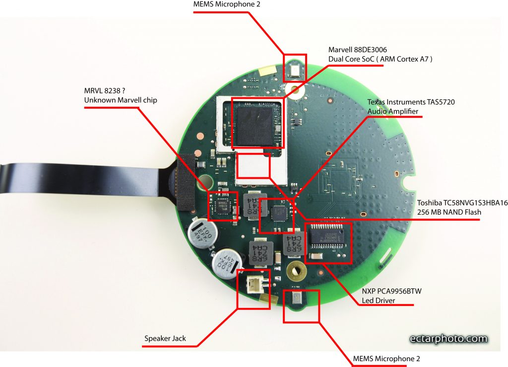
Bottom part of the main board
On bottom part we have main SoC, Audio amplifier, power circuit, Flash Memory and 2 MEMS microphones
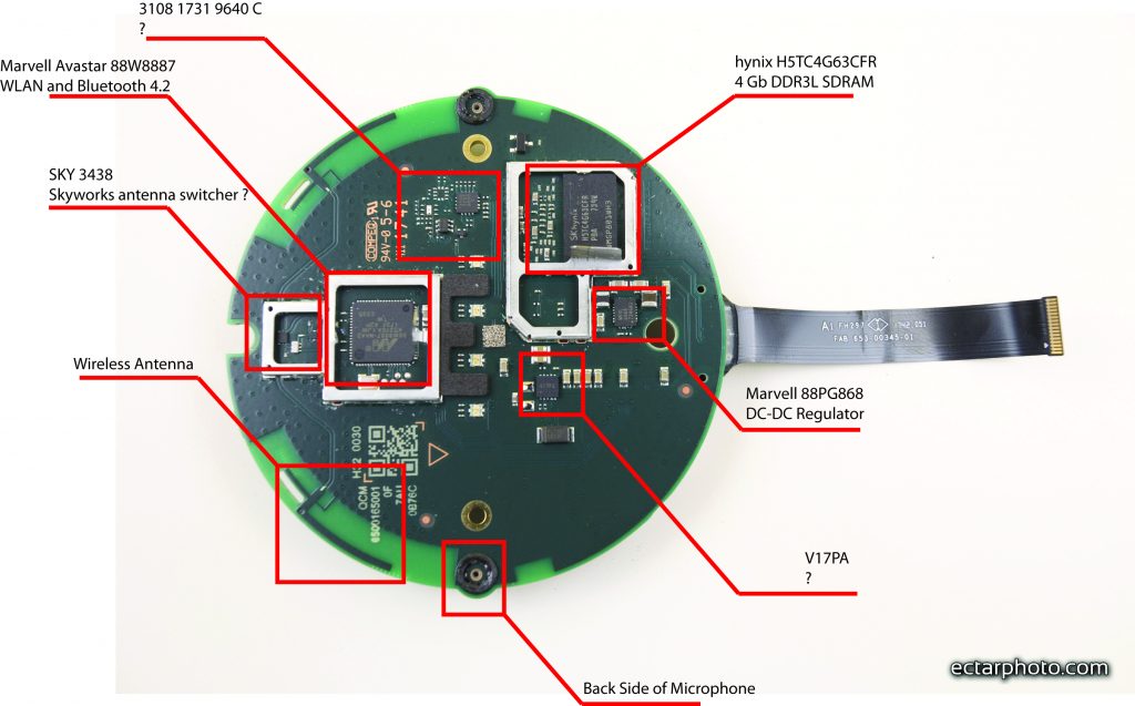
Top part of the main board
On top of the main board we have Marvels Wireless SoC ( WIFI, BT ), 512 MB of DDRL3 SDRAM, 4xLED and 2 unknown components.
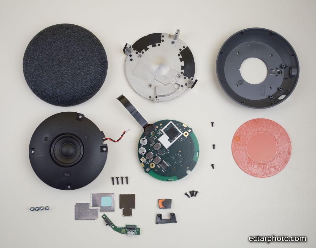
Here is complete photo of all components
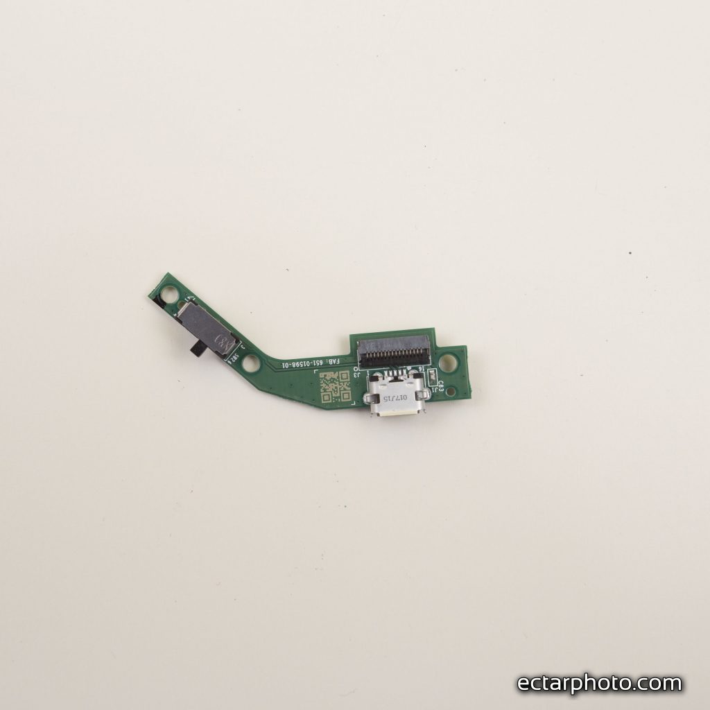
Close up of the switch and USB port board
List of main components:
TAS5720 – Audio amplifier from Texas Instruments. This is MONO power audio amplifier, at this point all dreams about having nice external audio from Google Home mini are shot. Data sheet is here: http://www.ti.com/lit/ds/symlink/tas5720m.pdf